Firmware
Description of the architecture design of the AMDS mainboard firmware.
Introduction
This document outlines the firmware architecture which runs the AMDS mainboard. By understanding how the mainboard works, users will be able to understand the performance limitations of the system. While the current firmware design will work for most applications, some users will find that the design must be tweaked to meet their system performance goals. Potential ideas for improvements are provided in the following sections which could be implemented in the future.
The main goal of the AMDS mainboard is to interface voltage/current sensor cards to an external control board (typically the AMDC). Therefore, the AMDS platform should be thought of as a slave to the main controller (master). The master must provide the signal to the AMDS that instructs it to sample all of the sensor cards. After all sampling is complete, the AMDS immediately transmits the latest sampled data back to master over two data lines.
Since the AMDS is typically used in motor drives, these operations happen in real-time at 1000s of times per second. To facilitate the desired real-time operation, the AMDS has an embedded processor which orchestrates its behavior. The firmware running on this processor directly determines the performance of the sensor interface in terms of sampling latency and throughput.
Architecture
While the architecture of the AMDS firmware is fairly simple, the I/O interface, priority of code, and latencies are critical to the overall performance.
Interface to Master
The AMDS firmware is designed to interface to the master controller over three logical wires: one signal from the master, and two data lines to the master. Physically, these signals are all differential pairs for noise immunity.


RX Signal: SYNC_ADC
The SYNC_ADC signal is used to trigger ADC sampling, which is followed by data transmission. This signal from the master should be a square wave. On each rising or falling edge, the AMDS samples all the sensor cards on the mainboard. Normally, the master triggers a transition on this RX signal when the PWM carrier is at a peak or valley. This synchronizes the ADC sampling to the inverter PWM, thus reducing sampling noise.
After all sensorcards have been sampled, the AMDS streams all sampled data back to the master (see below for data format).
TX Signals: DATA0 and DATA1
The two TX signals are controlled by the AMDS and go to the master. These are only used to send ADC sample data to the master. As soon as all ADCs are sampled, the AMDS starts sending the latest data to the master using the two TX wires. Two lanes are used so that the data can be transmitted at twice the speed, thus reducing latency.
The format of the data sent on the TX signals is UART. This means there is no clock line between the master and AMDS: the interface is completely asynchronous. The UART is configured to run at 20 Mbps. Conceptually, the TX lines are actually two distinct UART devices, each with only one-way communication. Both UARTs are configured as 8-bit data, 2 stop bits, and odd parity.
Data Format
The ADCs on the sensor cards are assumed to be 16-bit devices which are all compatible with each other (i.e. they can be daisy-chained and support equal clock rates). See each sensor card’s hardware design files for specs on the specific ADCs which are supported. The 16-bit raw data from the ADCs are packed into bytes which are sent across the DATA0 and DATA1 UART lines. DATA0 is used to send the contents of the first four sensor cards and DATA1 sends the last four sensor card data. The transmissions happen in parallel between the data lines.
The message structure is equal between both DATA0 and DATA1. However, each message corresponds to different sensor cards between DATA0 and DATA1 (i.e. 1-4, 5-8). Data is sent LSB first across the wire.
Packet 1: (first packet sent across DATAx line)
Byte 0 |
Byte 1 |
Byte 2 |
|---|---|---|
0x90 |
MSB of sample 1 |
LSB of sample 1 |
Packet 2:
Byte 0 |
Byte 1 |
Byte 2 |
|---|---|---|
0x91 |
MSB of sample 2 |
LSB of sample 2 |
Packet 3:
Byte 0 |
Byte 1 |
Byte 2 |
|---|---|---|
0x92 |
MSB of sample 3 |
LSB of sample 3 |
Packet 4: (last packet sent across DATAx line)
Byte 0 |
Byte 1 |
Byte 2 |
|---|---|---|
0x93 |
MSB of sample 4 |
LSB of sample 4 |
Note
There is no full CRC included in the transmission. The simple protocol relies on the parity check in the UART packet. This is not a terribly robust approach, but has worked well is moderate EMI environments.
Selective Channel Transmitting
To optimize processing and transmission bandwidth, the system supports disabling unused sensor channels.
Active Sensor Mask: The AMDS codebase contains a global variable active_sensor_mask that acts as a bitmask where 1 = Active and 0 = Inactive for each of the 8 AMDS sensor cards. This variable determines which sensor cards’ data are sent to the master each time a SYNC_ADC is received by the AMDS. For example,
active_sensor_mask = 0xFF;: AMDS will send all 8 channelsactive_sensor_mask = 0x01;: AMDS will only send sensor card channel 1active_sensor_mask = 0x06;: AMDS will only send sensor card channels 2 and 3
Hint
The AMDC platform system default is to send all 8 channels. If a reduced number of channels are being sent, the user must alert the AMDC to this by calling amdc_set_enabled(), as the AMDS does not communicate configuration settings with master.
Optimized Sample-and-Transmit Fast Path
The AMDS firmware has been optimized to minimize time from SYNC_ADC until the last bit of data is transmitted to the master. The code path used depends on the value of active_sensor_mask:
active_sensor_mask != OxFF: a generalized functionadc_sample_all_daughtercards()is used.active_sensor_mask == OxFF: a highly optimized functionadc_sample_and_transmit_fast_path()is used.
As compared to the generalized adc_sample_all_daughtercards() function, adc_sample_and_transmit_fast_path decreases latency by doing the following:
Avoid
active_sensor_maskConditional Checks: to remove processor time associated withifstatements.Hardware Cycle Counting: Rather than using
NOPloops for the 1300ns ADC wait time, the fast path uses the Cortex-M7 DWT Cycle Counter (DWT->CYCCNT) for deterministic waiting.Instruction Interleaving: The code optimizes wait states by starting SPI reads, and transmitting UART header bytes (
0x90) while the CPU is waiting for the SPI RX buffers to fill.
Both code paths optimize timing by using the ST32 MCU’s UART transmit shift register to queue up two bytes of UART transmit data at a time. This is done by optimizing calls to the inline drv_uart_putc_fast() function. When the shift register is empty, the function accepts new data without delay. When the shift register is occupied, the function blocks until it can take the new data byte. If the UART tranmit interface is idle, two back-to-back calls can be made to this function without any blocking delay.
Daisy Chain
The AMDS firmware includes support for up to three AMDS boards to be connected in series into a “daisy chain,” allowing for 24 sensor cards worth of data to be sent to master. Details of this are provided in AMDS Daisy Chain.
Interrupt-Driven Design
After start-up, the AMDS firmware is interrupt driven. This means that all critical processing occurs within an interrupt context, not the main loop. The interrupt which used to drive the firmware occurs on the rising and falling edges of the SYNC_ADC signal.
In the typical flow, the master is operating its PWM output and thus triggering the SYNC_ADC ISR periodically. The ADCs on the sensor cards start their conversions and store the latest data in the AMDS memory. Once this is complete, the AMDS sends the data back to the master. Then the AMDS will wait for the next SYNC_ADC interrupt.
Performance Limitations
The AMDS firmware design directly affects the operation limits of the SYNC_ADC signal. It will continue to work up to some threshold, at which point some ISRs will be missed and the performance will drop. However, the system will not “crash” – it will continue to work, albeit not as well.
The time for the trigger signal to reach the sensor card ADCs and for them to convert the analog value to digital is minimal, less than 1 µs. The time for the sensor cards to send their data back to the AMDS mainboard processor is around 3 µs. The latency for data transmission back to the master over the DATAx signals is about 9 µs. With all delays accumulated, the total time to trigger, sample, and transmit the data is just under 12 µs.
This can be seen in the timing block diagram and scope capture below.

The figure shown above assumes that the Timing Manager has been configured to sample the sensors only at the valley of the PWM triangle carrier, and attempts to sample every period (i.e., the sampling sub-rate ratio is 1). Also, note that in the figure, the AMDS sensor sampling time consumes about 90% of the total time slice—this leaves a very small time for the control code to run and does not represent practical configuration. Typically, the AMDS sampling time should consume much less of the total cycle time.
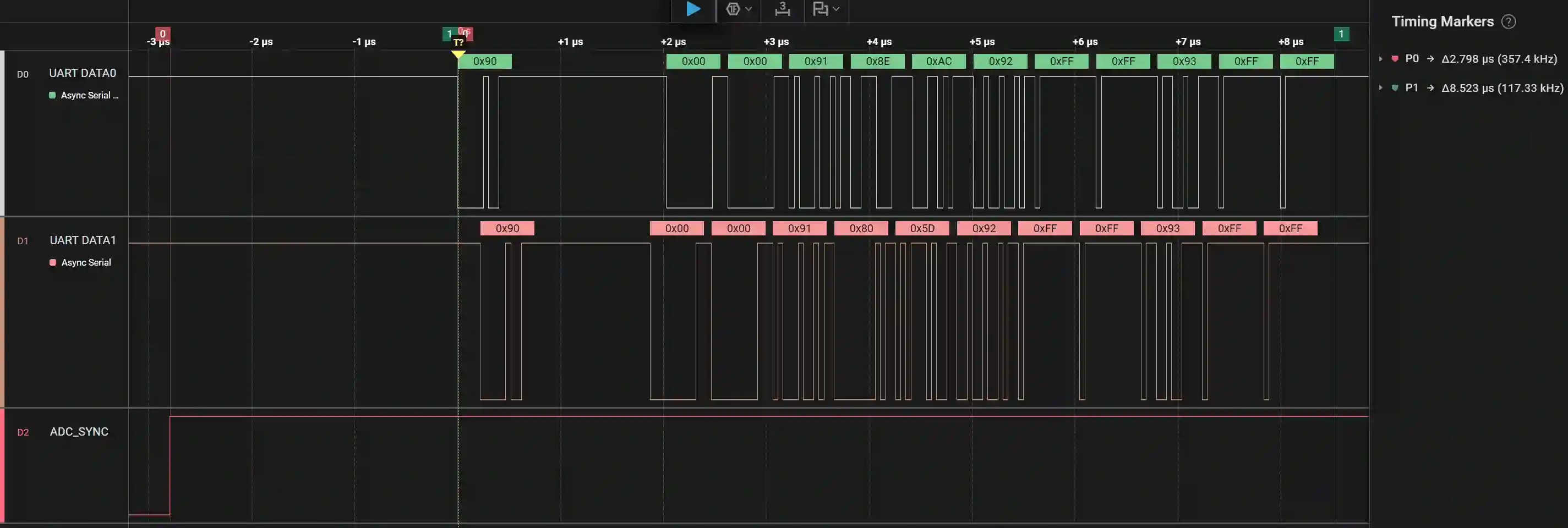
The channels in the above scope capture show the following signals from top to bottom:
UART DATA0: The
DATA0line from the AMDS back to the AMDC, showing 12 bytes (4 x 3-Byte packets) of UART data. This is the data for AMDS sensor card channels 1-4.UART DATA1: The
DATA1line from the AMDS back to the AMDC, showing 12 bytes (4 x 3-Byte packets) of UART data. This is the data for AMDS sensor card channels 5-8.ADC_SYNC: The
SYNC_ADCsignal from the AMDC to the AMDS, where every edge triggers the ISR on the AMDS which samples and returns the data.
Hint
The default value of active_sensor_mask will have the AMDS assume that all eight sensor cards must be sampled. Even when they are not populated, the firmware timing remains as if all sensor cards were in pairs of daisy chains. The only way to improve sample throughput when fewer cards are used is to update active_sensor_mask as described above.
Performance Specifications
Given a control frequency of Fs and PWM switching frequency of Fsw, the following constraints must be satisfied for the AMDS firmware to perform well:
Fsw<= 100kHz2 x
Fs<=Fsw
For application with SiC or GaN inverters where Fsw is typically much faster than Fs, the AMDS firmware works well.
Warning
When Fs is close to Fsw (i.e. control frequency is equal to PWM frequency), the current AMDS firmware design will not work well.
Future Improvements
The AMDS firmware works, albeit with limitations as described above. Some ideas to improve the system are now listed:
The AMDS cannot be configured from the master. Improvements could use an additional TX/RX pair to enable simple register protocol for config. This could be used to set digital filter bandwidths, turn on/off sensor card slots for faster sampling, etc.
The total sampling and data transmission latency as seen by the master (AMDC) could be improved. In the current firmware, the time from when the
SYNC_ADCline is toggled to when the newly sampled data has fully been received by the master is about 11 µs. This places limitations on the control rate of the master (AMDC). The improvements can come in several parts: 1) the actual ADC sampling time can be shorten by using theBUSYsignal from each ADC in an ISR to end the ADC sampling window. These are not used in the current firmware. Instead, the simpler approach of busy waiting until the max timeout occurs is used (i.e. wait for 1300 ns). However, the nominal wait time is only about 50% of this. 2) The data transmission time could be shorten by removing/reducing the overhead in the packet format, i.e., removing the header bytes.There is no robust CRC error detection on the data transmission from the AMDS to the master device, although the UART parity is used. Future improvements could add a footer CRC to ensure the received message at the master is valid. Error correction codes could also be used to further increase the communication robustness in high EMI environments (e.g. SECDED). There is no free lunch: all of these methods would increase the data transmission latency from the AMDS.