Low Voltage
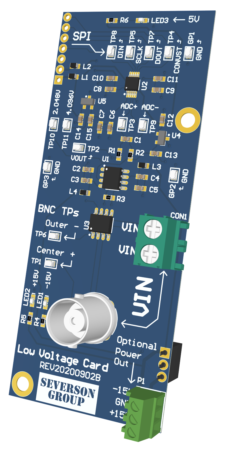
This document describes the design considerations and implementation details for the low voltage card, a sensor card for the AMDS mainboard.
Relevant Hardware Versions
REV A
REV B

Design Requirements and Considerations
The analog input card was designed to the following specifications:
Analog input signal of +/- 10V
Truly differential input
High common-mode rejection ratio
ADC has various pin-compatible versions available (different sampling rates)
Since these requirements very closely mirror the analog inputs on the AMDC, a similar design is used. The reader can learn about the AMDC analog inputs by reading its documentation. The same front-end analog conditioning circuitry is used. However, while the ADC is still a differential input device (like the AMDC), it is a different part. This analog input board has a single-channel 16-bit ADC that accepts differential inputs. The digital interface is standard SPI.
Various ADCs are available which are pin-compatible to the part designed into the PCB. This means that the user can select which one they want when they assemble the boards. The ADCs offer the same specs, but vary on the sample rate. More expensive ADCs provide a higher sample rate.
Relationship Between Input and ADC voltage
For both REV A and REV B low-voltage sensor boards with \(V_{\rm REF}\) = 2.048V, the relationship between the input voltage \(V_{\rm IN}\) and the ADC input voltage \(V_{\text{ADC}}\) is given by:
Pin Compatible ADCs
The default ADC is bolded below, but any of the follow ADCs work with the design.
100 kSPS: ADS8867
400 kSPS: ADS8865
680 kSPS: ADS8863
1000 kSPS: ADS8861